At the end of this session you should be able to:-
1) draw a schematic using OrCAD Capture CIS.
2) do the finishing to the schematic to create a printed circuit board (PCB)
DRAWING SCHEMATICS
1. To begin, choose Capture CIS program from your desktop, select options
File>New>Project as shown in the figure below.
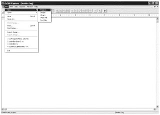
Figure 1.1: The initial window of OrCAD Capture
2. This option will invoke the New Project dialog box, as shown in Figure 1.2
below.You should name your project as PCB1_yourname, and create new project
using PC Board Wizard and create your own directory as shown in Figure 1.3.
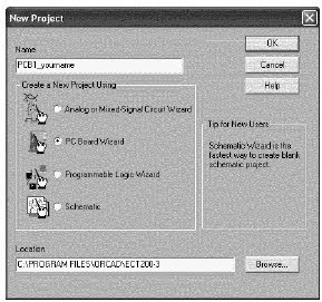
Figure 1.2: New Project dialog window
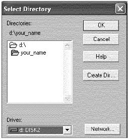
Figure 1.3: Select directory window
3. Then, dialog box as shown in figure below displays, just click Next to
continue.
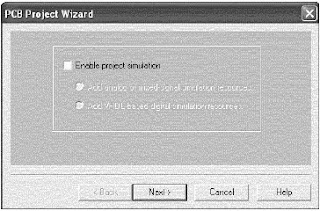
Figure 1.4: PCB Project Wizard
4. The next step is to load libraries of parts which will be available to you when
you are drawing the circuit schematics. The dialog box is for adding and
removing libraries is shown Figure 1.5 below. You might add or remove the
libraries later,now click Finish and continue to draw the schematic.
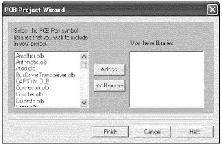
Figure 1.5: Add or remove libraries dialog box
5. Draw the circuit as shown in the Figure 1.6 below.
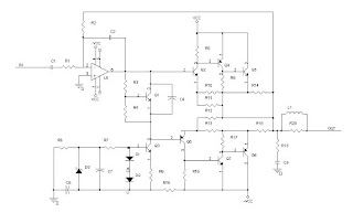
Figure 1.6: Schematic of an audio amplifier circuit
6. When finish draw the schematic, select all component from the Edit menu or by
pressing Ctrl+A. Then, from Edit menu, click Properties or Ctrl+E to edit the
properties of all the parts. The window as in figure below appears. Choose
filter by Layout. Select Parts tab.
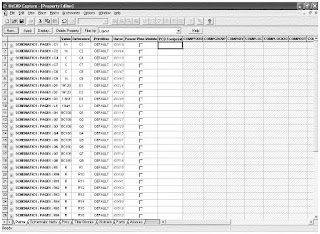
Figure 1.7: Property Editor window
7. Refer to Appendix A given, enter the appropriate footprint for each one of the
parts in the schematic as shown in figure below. Click the PCB footprint cell
for any one of the parts, type the footprint name. Notice that you must
recognize physically how the parts look like in order to specify their correct
footprint.
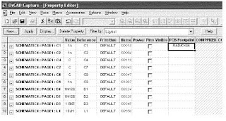
Figure 1.8: Specify a PCB footprint
FINISHING SCHEMATICS
1. Now, displays the Capture’s project manager window, click schematic page as
shown in the figure below.
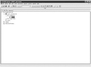
Figure 1.9: Project Manager window
2. the design by choosing Tools>Annotate or by clicking the toolbar. This is for
update the part reference to prepare the netlisting. Annotate menu window will
appear as shown below. Click OK to annotate. Another dialog appears as shown in
figure 1.11. Click OK to continue.
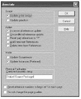
Figure 1.10: Annotating design

Figure 1.11
3. The design must be check for multiple parts of same reference or invalid
package or nets. Design Rules Check (DRC) will do this. Choose Tools>Design
Rules Check or clickbutton from the toolbar. DRC menu as shown below appear. If
there are errors, dialog box such in figure 1.13 will appear.
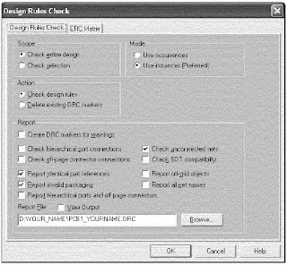
Figure 1.12: DRC
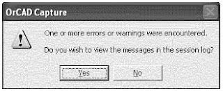
Figure 1.13: Error in DRC
4. If DRC does not give any error, proceed by creating netlist for PCB Layout. If
otherwise, you must identify and fix the problems.
5. To create netlist for PCB, choose Tools>Create Netlist or clickbutton from
the toolbar. Netlist menu as shown below display. Select the desired netlist
type by clicking the Layout tab. Click OK to create netlist. Save your design
by clicking OK for the next dialog box.
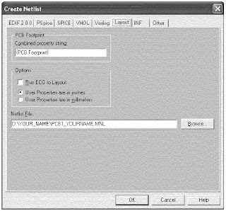
Figure 1.14: Create netlist for the design
6. Close and save your design.
0 comments:
Post a Comment